

Research
Research News
Total 83
-
Splitting water molecules for a greener future? Design of a nove...
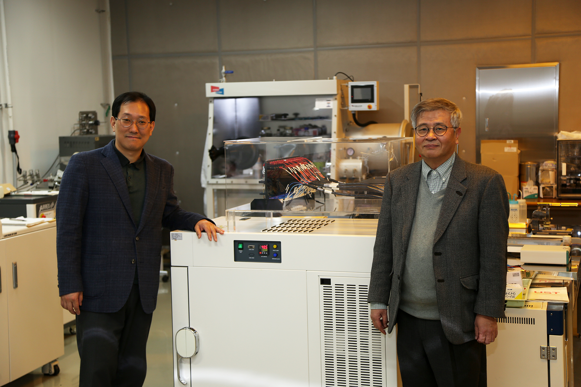
Splitting water molecules for a greener future?Design of a novel catalystShort description:Scientists at Dongguk University developed a novel nickel-based hydroxide compound that can be used as a powerful catalyst for the electrolysis of water. This material could be useful for developing renewable energy sources. Nowadays, people acknowledge the importance of finding and improving renewable energy sources. One strategy to generate energy is breaking water molecules (H2O) apart in an electrochemical reaction known as electrolysis. This process allows us to convert energy from the sun or other renewable sources into chemical energy. However, electrochemically splitting water molecules requires an overpotential—an excess voltage that has to be applied in addition to the theoretical voltage (1.23 V vs reversible hydrogen electrode or RHE) so that the necessary reactions can occur.Electrocatalysts are materials that, because of their electrical and morphological features, facilitate electrochemical processes. Researchers have been searching for electrocatalysts that can aid in the electrolysis of water, and some of the best catalysts are noble-metal oxides, which are rare and costly. Nickel-based hydroxide (Ni(OH)2) compounds are, fortunately, a better alternative. A team of scientists, including Profs. Hyunsik Im and Hyungsang Kim from Dongguk University, intercalated polyoxovanadate (POV) nanoclusters into Ni(OH)2 arranged in ordered layers and found that doing this improves its conducting and morphological properties, which in turn enhances its catalytic activity. They employed a promising method called chemical solution growth (CSG), wherein a highly saturated solution is prepared, and the desired material structure naturally forms as the solutes precipitate in a predictable and controlled fashion, creating a layer-by-layer structure with POV nanoclusters intercalated between the Ni(OH)2 layers.The team demonstrated that the resulting house-of-cards-like structure greatly reduced the overpotential needed for the electrolysis of water. They attributed this to the morphological features of this material; the POV nanoclusters increase the spacing between the Ni(OH)2 layers and induce the formation of micropores, which increases the surface area of the final material and the number of catalytic sites where water molecules can be split. “Our results demonstrate the advantages of the CSG method for optimizing the pore structure of the resulting material,” explains Prof. Im. Facilitating the electrolysis of water using novel catalysts is a step toward achieving a greener future. What’s more, the CSG method could be useful in many other fields. “The facile CSG deposition of nanohybrid materials may be useful for applications such as the production of Li-ion batteries and biosensors,” states Prof. Kim. Only time will tell what new uses CSG will find.ReferenceAuthors:Jayavant L. Gunjakar1,2, Bo Hou3, Akbar I. Inamdar1, Sambhaji M. Pawar1, Abu Talha Aqueel Ahmed1, Harish S. Chavan1, Jongmin Kim1, Sangeun Cho1, Seongwoo Lee1, Yongcheol Jo1, Seong-Ju Hwang4, Tae Geun Kim5, SeungNam Cha3, Hyungsang Kim1*, and Hyunsik Im1*Title of original paper:Two-Dimensional Layered Hydroxide Nanoporous Nanohybrids Pillared with Zero-Dimensional Polyoxovanadate Nanoclusters for Enhanced Water Oxidation CatalysisJournal:Small DOI:10.1002/smll.201703481Affiliations:1Division of Physics and Semiconductor Science, Dongguk University 2D. Y. Patil Education society 3Department of Engineering Science, University of Oxford 4Center for Intelligent Nano-Bio Materials (CINBM), Department of Chemistry and Nano Sciences, Ewha Womans University 5School of Electrical Engineering, Korea University*Corresponding author’s email: H. Kim (hskim@dongguk.edu); H. Im (hyunsik7@dongguk.edu) About Dongguk UniversityDongguk University, founded in 1906, is located in Seoul, South Korea. It comprises 13 colleges that cover a variety of disciplines and has local campuses in Gyeongju, Goyang, and Los Angeles. The university has 1,300 professors who conduct independent research and 18,000 students undertaking studies in a variety of disciplines. Interaction between disciplines is one of the strengths on which Dongguk prides itself; the university encourages researchers to work across disciplines in Information Technology, Bio Technology, Culture Technologys, and Buddhism. About the authorProf Hyungsang Kim and Prof Hyunsik Im completed their PhD and D.Phil degree from Kӧln in 1994 and from Oxford in 1999 respectively, and are currently full time academicstaff in the department of Physics and Semiconductor Science, Dongguk University, Seoul, South Korea.
2019.01.10. 조회 4150 -
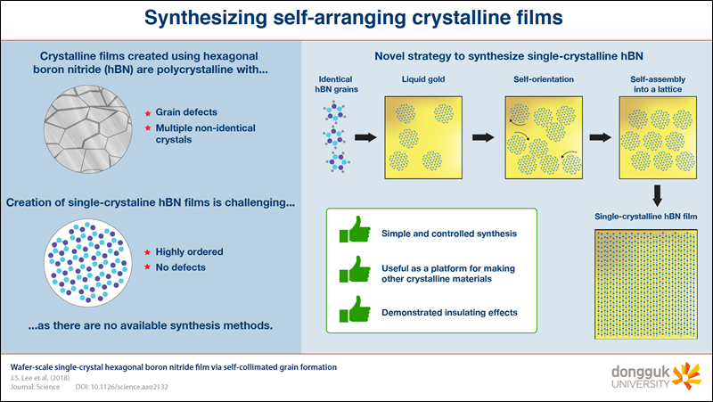
Synthesizing crystalline films that neatly arrange themselves
Synthesizing crystalline films that neatly arrange themselvesScientists at Dongguk University (Prof. Ki Kang Kim) in collaboration with scientists from other institutes (KIST (Dr. Soo Mim Kim), Sungkyunkwan University (Prof. Young Hee Lee) found a method for synthesizing hexagonal boron nitride films with a nearly perfect single-crystalline structure. This structure consistently self-assembles on top of liquid gold and can be used as a platform for synthesizing other crystalline thin-film materials. Crystalline structures are ideally composed of repeating identical units in a perfectly ordered fashion. As one would expect, crystals have found applications in a multitude of fields, such as optics, electronics, and chemistry, and have helped researchers understand the mechanics behind complex physical phenomena. However, synthesizing perfect crystalline structures is very challenging, with most methods yielding crystals with defects or with multiple different basic units (called polycrystals).Hexagonal boron nitride (hBN), also called white graphite, can be synthesized in the shape of crystalline films with the width of a single atom. They have an insulating effect that has found uses in various types of scientific research. However, these films are polycrystalline and not single-crystalline. Therefore, a research team set out to find a method for synthesizing single-crystalline hBN films on a small scale.The synthesis method they developed consists of letting the thin hBN film self-assemble on top of a liquid gold substrate. Because of the surface tension of liquid gold and the characteristics of its interaction with boron and nitrogen, circular hBN grains form automatically over time. These grains grow to a specific diameter and eventually form a lattice. They can easily rotate when they are about to come into contact with another grain so as to assume the best possible orientation before joining the lattice (ref. video:https://www.youtube.com/watch?v=NI1ZhI0Qml8&feature=youtu.be) The final product of this process is a nearly perfect single-crystalline hBN film, as the team demonstrated in many different experiments and via multiple measurements. A very promising application of such films is using them as a substrate for synthesizing other crystalline thin-film materials on top of them, such as graphene. Their applications go beyond that, as Prof. Kim explains, “We demonstrated that our hBN films can serve as a protecting layer against metal oxidation and as a gas-diffusion barrier for water vapor transmission.”This innovative synthesis method could be exploited further as well. “Our strategy for the synthesis of single-crystalline hBN films opens a new horizon for the single-crystal growth of other diatomic 2D materials,” explains Prof. Kim. This would make many single-crystalline materials easier to fabricate, allowing them to naturally find a multitude of applications. ReferenceAuthors:Joo Song Lee1,2, Soo Ho Choi3, Seok Joon Yun4, Yong In Kim5, Stephen Boandoh6, Ji-Hoon Park4,5, Bong Gyu Shin4,7,8, Hayoung Ko1,5, Seung Hee Lee2, Young-Min Kim4,5, Young Hee Lee4,5*, Ki Kang Kim6*, Soo Min Kim1*Title of original paper:Wafer-scale single-crystal hexagonal boron nitride film via self-collimated grain formationJournal:ScienceDOI:10.1126/science.aau2132Affiliations:1Institute of Advanced Composite Materials, Korea Institute of Science and Technology (KIST)2Applied Materials Institute for BIN Convergence, Department of BIN Fusion Technology and Department of Polymer-Nano Science and Technology, Chonbuk National University 3Department of Physics, Dongguk University-Seoul 4Center for Integrated Nanostructure Physics (CINAP), Institute for Basic Science (IBS) 5Department of Energy Science, Sungkyunkwan University 6Department of Energy and Materials Engineering, Dongguk University-Seoul 7Center for Quantum Nanoscience (QNS), Institute for Basic Science (IBS), Ewha Womans University 8Department of Physics, Sungkyunkwan University *Corresponding author’s email:kkkim@dongguk.edu, kkkim@dongguk.edu, kkkim@dongguk.edu About Dongguk UniversityDongguk University, founded in 1906, is located in Seoul, South Korea. It comprises 13 colleges that cover a variety of disciplines and has local campuses in Gyeongju, Goyang, and Los Angeles. The university has 1,300 professors who conduct independent research and 18,000 students undertaking studies in a variety of disciplines. Interaction between disciplines is one of the strengths on which Dongguk prides itself; the university encourages researchers to work across disciplines in Information Technology, Bio Technology, Culture Technologys, and Buddhism. About the authorDr. Ki Kang Kim received his M.S. and Ph.D. from the Department of Physics of Sungkyunkwan University, Republic of Korea, in 2008 under the supervision of Prof. Young Hee Lee. After completing his postdoctoral studies under the supervision of Prof. Jing Kong at Massachusetts Institute of Technology, USA, he joined the Department of Energy and Materials Engineering at Dongguk University in Republic of Korea in 2012 as an assistant professor. His current research interests include the synthesis of 2D materials and engineering the electronic structure of low-dimensional materials.
2019.01.10. 조회 2926 -
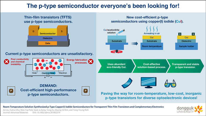
Semiconductor for making the thin-film transistors that everyone...
Semiconductor for making the thin-film transistors that everyone’s been looking for!Scientists at Dongguk University have found a way to create printed p-channel thin-film transistors by using the abundantly available and environmentally friendly copper(I) iodide semiconductor at room temperature. Their energy-efficient and cost-effective fabrication method for these transistors may pave the way for developing low-cost and novel optoelectronic devices. Transistors are the building blocks of most of the electronic devices we use every day, and research on fabricating new types of semiconducting materials for thin-film transistors (TFIs) has been ongoing for decades. Whenever new transistors or novel fabrication methods are discovered, many previously impossible applications become feasible, such as ultrahigh-definition transparent displays and flexible electronic devices. Nowadays, there is a huge demand for p-type transparent semiconductors (which are conductive due to the movement of charge carriers called “holes”) for making p-channel transistors, but when compared to the n-type counterparts, their use is limited by chemical instability and poor electric properties. To overcome these limitations, a research team at Dongguk University led by Prof. Yong-Young Noh focused on developing a p-type transparent semiconductor for TFTs using a metal halide like copper(I) iodide (CuI), instead of metal oxide. “The naturally abundant and environment friendly constitutional elements of CuI make it more appropriate for large-scale printed transparent electronics. More importantly, CuI has a higher hole mobility than other p-type oxide-based semiconductors,” explains Prof. Noh.However, CuI had been barely used as a semiconductor for TFTs because its hole concentration is so high that it results in uncontrollable conductivity (transistors are generally meant to be easily turned on and off at high speeds, that is, they are meant to be switchable from a conductive to a non-conductive state). Moreover, standard solution-based processing for making thin films generally requires a heat treatment called “annealing,” which is energy and time consuming.The researchers found out that it is possible to reduce the conductivity of CuI-based thin films by making them even thinner and thus suitable for fabricating TFTs with the performance that is currently in demand for many applications. Additionally, these CuI thin films do not require annealing at all and can be processed at room temperature. This saves energy and makes them more cost-effective. The team tested multiple processing conditions and fabricated various different TFTs to determine the origin of the enhanced device properties and to demonstrate the potential uses of CuI as a thin-film p-type semiconductor. “We believe that this work opens the floodgate for room-temperature, low-cost, printed transparent p-type transistors for diverse optoelectronic devices,” concludes Prof. Noh.ReferenceAuthors:Ao Liu1, Huihui Zhu1, Won-Tae Park1, Seok-Ju Kang1, Yong Xu*1, Myung-Gil Kim*2, and Yong-Young Noh*1Title of original paper:Room-Temperature Solution-Synthesized p-Type Copper(I) Iodide Semiconductors for Transparent Thin-Film Transistors and Complementary Electronics Journal:Advanced Materials DOI:10.1002/adma.201802379Affiliations:1Department of Energy and Materials Engineering, Dongguk University 2Department of Chemistry, Chung-Ang University*Corresponding authors’email:yynoh@dongguk.eduAbout Dongguk UniversityDongguk University, founded in 1906, is located in Seoul, South Korea. It comprises 13 colleges that cover a variety of disciplines and has local campuses in Gyeongju, Goyang, and Los Angeles. The university has 1300 professors who conduct independent research and 18000 students undertaking studies in a variety of disciplines. Interaction between disciplines is one of the strengths on which Dongguk prides itself; the university encourages researchers to work across disciplines in Information Technology, Bio Technology, CT, and Buddhism.
2019.01.10. 조회 2162
- Seoul Campus
- 30, Pildong-ro 1-gil, Jung-gu, Seoul, 04620, Republic of Korea
- Tel +82-2-2260-3314 Fax +82-2-2260-2277
- incoming@dongguk.edu (Exchang Program)
- scf@dongguk.edu (International Students Services)
- adm@dongguk.edu (International admission)
-
cscenter@dongguk.edu
(Certificate Issuance, Education Verification) - kic@dongguk.edu (Korean Language Course)