Researchers developed a novel optoelectronic memory device that addresses the issues of conventional floating-gate nonvolatile memory devices.
Despite rapid progress, conventional floating-gate nonvolatile memory devices still face critical challenges. Optoelectronic memory devices (OEMs) based on two-dimensional (2D) van der Waal heterostructures (vdWhs) are a promising solution but suffer from reliability and endurance issues. Addressing these shortcomings, researchers have developed a novel rhenium selenide and 2D tellurene-based vdWh with multilevel storage capabilities, marking a significant step in OEM development.
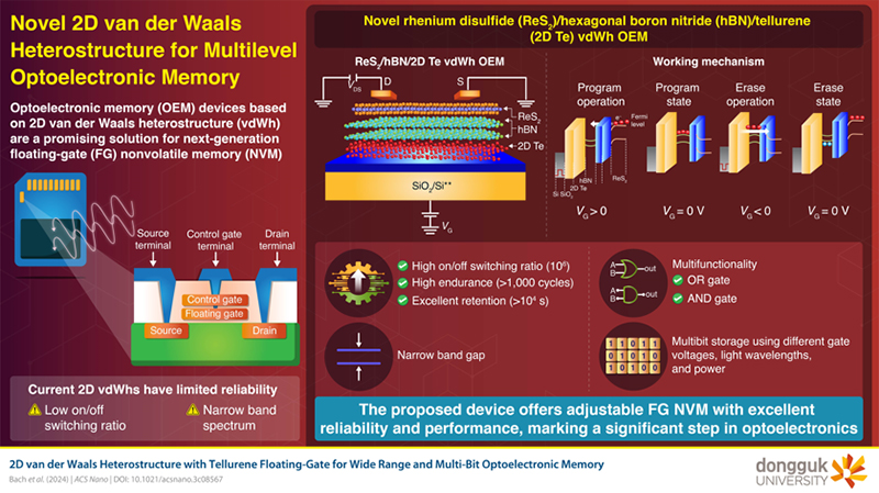
Image title: Operation of the optoelectronic memory device with telluride floating-gate
Image caption: The novel optoelectronic memory device exhibits impressive stability and a broad adsorption spectrum, and is capable of multi-bit storage, marking a significant step in floating-gate nonvolatile memory technology.
Image credit: Hyunsik Im from Dongguk University
License type: Original Content
Usage restrictions: Cannot be reused without permission
Floating-gate (FG) nonvolatile memory technology has witnessed rapid development in recent years, offering several advantages in areas like the Internet of Things, multilevel data storage, and next-generation flash memory. Despite this progress, critical challenges such as reducing memory cell size and power consumption are still not solved.
A promising solution to these challenges lies in optoelectronic memory (OEM) devices, which can convert light to electricity and vice versa, based on two-dimensional (2D) van der Waal heterostructures (vdWhs). These heterostructures are composed of 2D material layers stacked in a precise order with weak inter-layer bonds, endowing them with unique optoelectrical properties. Previous studies have explored vdWh OEMs using different materials, including graphene, black phosphorous, and perovskite. However, these devices suffer from narrow light absorption spectrums, low on-off switching ratios, and low data retention, limiting their long-term use and reliability.
To address these problems, a team of researchers from Dongguk University, Korea, led by Professor Hyunsik Im from the Division of Physics and Semiconductor Science, has developed a novel high-performance OEM based on rhenium disulfide (ReS2)/hexagonal boron nitride (hBN)/tellurene (2D Te) vdWh. Their findings were made available online on January 11, 2024, and published in Volume 18, Issue 05 of the journal ACS Nano on February 06, 2024.
The researchers fabricated the OEM device by stacking a few layers of ReS2 on top of a hBN layer followed by a 2D Te FG, all on a silicon dioxide substrate. Tests revealed that the ReS2/hBN/2D Te vdWh device exhibits exceptional long-term stability, a high on/off switching ratio of the order of 106, and impressive data retention, owing to the excellent optoelectrical properties of ReS¬2 and 2D Te. Moreover, it also demonstrated a broad absorption spectrum extending from the visible to near-infrared region at room temperature.
Expanding on the results, Prof. Im says, “Our device can achieve multi-bit storage states by varying the gate voltage, input laser wavelength and laser power, enabling complex data patterns and high data capacities.” Furthermore, the device can perform fundamental OR and AND Boolean logic gate operations, crucial for digital circuits, by combining electrical and optical inputs.
“Our research marks a significant milestone in multi-bit optoelectronic memory technology, holding great potential in various applications, including artificial intelligence systems, cloud computing, and broadband optical programmability for digital circuits,” concludes Prof. Im.
Reference
Title of original paper: 2D van der Waals Heterostructure with
Tellurene Floating-Gate for Wide Range and
Multi-Bit Optoelectronic Memory
Journal: ACS Nano
About Dongguk University
Dongguk University, founded in 1906, is located in Seoul, South Korea. It comprises 13 colleges that cover a variety of disciplines and has local campuses in Gyeongju, Goyang, and Los Angeles. The university has 1300 professors who conduct independent research and 18000 students undertaking studies in a variety of disciplines. Interaction between disciplines is one of the strengths on which Dongguk prides itself; the university encourages researchers to work across disciplines in Information Technology, Bio Technology, CT, and Buddhism.
About Professor Hyunsik Im
Hyunsik Im is currently a Professor at the Division of Physics and Semiconductor Science, at Dongguk University, Seoul, Korea. He obtained his D.Phil. degree in Physics at the University of Oxford. His research interests lie in fabrication and electrical transport in nanodevices at low temperatures. His group is also developing approaches for X-ray scintillators and optoelectronic and energy storage devices.
About Dr. Duc Anh Nguyen
Dr. Duc Anh Nguyen received the Ph.D. degree at Department of Energy Science, Sungkyunkwan University, Suwon, Korea. He is working as a Research Assistant Professor in the Division of Physics and Semiconductor Science, Dongguk University, Seoul, Korea. His research is currently the synthesis and application of 2D materials for optoelectronic and memory devices.
About Thi Phuong Anh Bach
Thi Phuong Anh Bach is currently studying Ph.D. program at the Division of Physics and Semiconductor Science, Dongguk University, Seoul, Korea. Her research focuses on the two-dimensional materials and their heterostructures for optoelectronic devices.

